
As artificial intelligence, cloud computing, and data-intensive applications continue to grow, the demand for faster and more energy-efficient computing has never been higher. IBM may have just taken a major step toward meeting that challenge with its groundbreaking sub-1 nanometer chip technology.
Recently, IBM unveiled the world’s first 0.7nm (7 angstrom) chip architecture, pushing semiconductor innovation beyond the current limits of chip design. While still in the research stage, this breakthrough could redefine how future processors deliver performance while reducing energy consumption.
What Makes IBM’s Sub-1nm Chip Different?
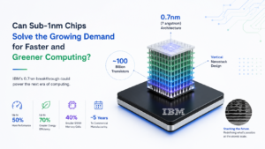
Unlike traditional chips that place transistors side by side on a flat surface, IBM’s new design uses a vertical “nanostack” architecture. By stacking transistors in three dimensions, the company can fit approximately 100 billion transistors onto a chip roughly the size of a fingernail.
This approach offers two significant benefits:
- Up to 50% higher performance compared to previous 2nm chip designs.
- Up to 70% better energy efficiency, helping reduce power consumption across data centers, AI workloads, and consumer devices.
IBM also reports that the new architecture can shrink logic-based memory circuits (SRAM) by nearly 40%, creating more space for advanced processing capabilities.
Why This Matters for Sustainable Computing
The rapid growth of AI and cloud infrastructure is driving energy consumption to unprecedented levels. Data centers already account for a significant share of global electricity usage, and demand is expected to rise as AI adoption accelerates.
Sub-1nm chips could help address this challenge by delivering more computing power while using less energy. For businesses, that means lower operating costs. For consumers, it could translate into longer battery life and faster devices. For the environment, it represents a meaningful step toward greener computing.
When Can We Expect These Chips?
Although IBM has successfully demonstrated the technology in a laboratory environment, commercial adoption is still a few years away. The company estimates that sub-1nm chips could reach manufacturing and mainstream use within the next five years.
While challenges remain, IBM’s breakthrough highlights the future direction of semiconductor innovation—smaller, faster, and significantly more energy efficient.
The Bottom Line
IBM’s sub-1nm chip technology isn’t just another incremental upgrade. It represents a potential leap forward in solving one of the industry’s biggest challenges: delivering higher performance without increasing energy consumption. If the technology scales successfully, it could play a key role in powering the next generation of AI, cloud computing, and sustainable digital infrastructure.